.png)

Miniaturization entails a wealth of possibilities for progress in many industries, where the demand of innovative and miniaturization solutions is constantly increasing. Innovative assembly techniques, equipment, processes and expertise are needed to tackle the challenges and push the limits of miniaturization.
The trend toward miniaturization has been redirected to a new approach which goes beyond the simple size reduction of components.
Read the whole article to discover the most innovative miniaturization processes and their benefits and challenges in their implementation.
Miniaturization nowadays
Until recently, miniaturization in electronics has fully relied on components reduction in their size, but this miniaturization always reach obvious limitations. To simply illustrate those limits, think of folding a piece of paper in half. You have now reduced the surface space of 50% through the process of folding. However, if you keep folding the paper in half, at some point you won't be able to fold the paper anymore and the folding process breaks down. Thus, to make that piece of paper even smaller, you must change the process and try a new one: for instance by breaking out your scissors and cut the folded paper in half. The size of the paper is still reduced, but through a different method. Turning back to miniaturization in the electronic industry, the same logic has been applied. Today another approach for miniaturization has been adopted, which is called miniaturization through modular integration.
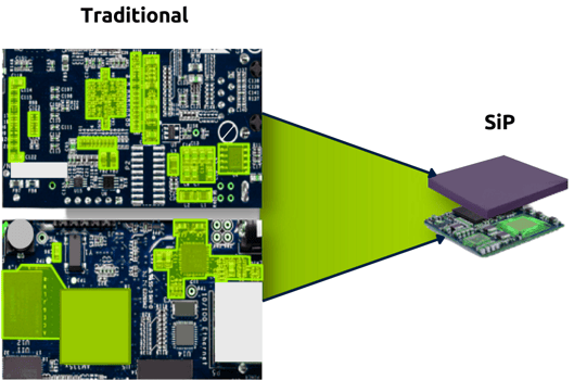
Essentially, modular integration means integrating multiple integrated circuits (ICs), active and passive components in a single compact package to produce a System in a Package (SiP) where all components work together. This approach has even greater potential for size reduction than simply relying on semiconductor developments. In such SiPs, circuits are very dense and are developed with narrow traces and spaces, by placing small components very close in a precise manner, as well as partitioned in a different way, in order to deliver the same capabilities but using less components. Here an example of a traditional circuit developed using the SiP innovative process:
Generally, miniaturization was driven by mobile phones, which over time increasingly became smaller and flatter, but nowadays miniaturization is raising demand in many sectors. The aerospace industry, military and defense, medtech and the big industry of consumer electronics miniaturization are constantly looking for innovative solutions which can be miniaturized as much as possible. Wearables are one of the most flourishing markets in the consumer goods sector, think to smart watches, which are able to measure and record data about health and fitness, reading emails and messages, to wireless earbuds with high sound quality and noise canceling functions, or again to most recent innovations like smart glasses able to take photographs, record videos and support augmented reality, which are just about to enter the market. Not to mention medical monitoring devices and automotive subsystems, which are extremely dependent from miniaturization.
With the growing interest in wearables, medical devices and automotive systems, and the ongoing objective of developing always smaller and smaller smart devices, technology will increasingly go hand in hand with miniaturization which is sure to increase further, especially thanks to a SiP approach.
Benefits of miniaturization
With no doubts miniaturization represents a key value for the technology progress, and the competitive race to develop always smaller, thinner and lighter devices, without losing performance and functionality, has driven and is still driving many tech markets.
Miniaturization has the obvious advantage of size reduction, but benefits are not limited to that. As expert in the electronic industry, we analysed the main advantages of being up-to-date with the most cutting-edge solutions:

MORE SPACE FOR BATTERIES
Miniaturization of electronic components allow to free up space which can be used to increase the efficiency of a device. For instance, batteries are usually the bulkiest in a device but are very important to guarantee a certain autonomy. Hence, further space is useful for the incorporation of larger batteries without increasing the overall size of a device.

THERMAL PERFORMANCE
Well implemented SiPs also offer excellent thermal performance combined with high reliability thanks to their encapsulation, which provides comprehensive protection against the external environment.
.png?width=153&name=24%20-%20Copia%20(3).png)
MODULAR SiPs
In various applications, modular integration of carefully designed SiPs can offer a simplified product design and reduces inventory, as well as it allows to save time and money since the SiP has to be tested, approved and qualified only one time.
.png?width=153&name=24%20-%20Copia%20(2).png)
BETTER SIGNAL
Miniaturization means greater density of circuits and components closeness. This, in turn means shorter signal paths which enable higher frequencies and clock rates.

STYLE OF THE END PRODUCT
For end products, especially in consumer goods, aestethics is also very important. Smaller modules give designers more freedom and flexibility to produce more stylish products to ensure consumer appeal.
Given the many benefits, the potential improvements in terms of miniaturization are almost limitless, and various application areas will create further demands for miniaturized solutions.
Overcome the challenges with a reliable EMS partner
With the numerous benefits, different challenges and limitations come along as well. Scaling-down devices is neither simple nor effortless. Integrating more functionalities into smaller devices brings many challenges in terms of design, development and volume manufacturing. From the accurate placement of the smallest components to the requirement of designing customized hybrid and high-density components, the main challenge lays in innovating while keeping test and manufacturability in mind. Due to these challenges, taking advantage of the multiple benefits of the latest advances in miniaturization is not easy and businesses are often under strain because of the lack of experience. Here the three main challenges you need to be aware of:
- Miniaturized components procurement: supply chain managers may struggle to find the components they need for miniaturized electronic components assemblies to be produced in house. This requires high expertise in the electronic industry and in the capability of finding alternatives every time a component is not available on the market, especially during current component shortages.
- Assemblying high-density PCBs: the challenges in the assembly phase are inversely proportional to the size of the components used to populate the boards. At reduced sizes, components can get extremely difficult to rework and boards that cannot be reworked have a significant impact on the manufacturing performance. Thus, it is highly important for electronic manufacturers to have equipment and machinery that can handle it.
- Expertise in manipulating components assembly: reducing PCBs' size is also challenging when it comes to layout design as well. To accommodate the maximum number of components, engineers have to challenge the IPC specifications and should be able to manipulate the assembly of the components. Innovative layout techniques have to be developed to layout a high speed circuit while keeping the signal integrity intact.
To mitigate the risks and efficiently overcome the above mentioned challenges, the selection of the right EMS company becomes crucial for the development and manufacturing of your electronic device.
Hemargroup miniaturization solutions
Given the various benefits of this new approach of SiPs, companies enthusiastically embrace miniaturization in their new product development programs to become more profitable and to be innovative. However, a smooth progress largely if not completely depends on finding the right EMS partner to support the development, the implementation and the manufacturing of miniaturized solutions. The design of such solutions requires engineering expertise to achieve the desired functionality, but also ensuring optimum thermal and Electromagnetic compatibility (EMC) performance while maximizing power economy. Software expertise is also needed to reap the benefits of programmable devices. Last but not least, a proper EMS partner must dispose of capable manufacturing facilities with highly sophisticated machinery and equipment.
Hemargroup is an international EMS company based in Switzerland with 50 years of experience in contract electronic design, prototyping, production, industrialisation, and manufacturing, up to mass scale, of electronic components and end products in many high-tech industries. The quality of our processes is the heart of our strategy and our main goal is to offer the best possible service through the whole product lifecycle, comprehensive of miniaturization solutions. Our own production site and all processes and procedures are ISO and IPC certified. We are certified ISO9001 for quality management, ISO14001 for environmental management, AQAP 2110 for development and production of military devices, and ISO 13485 for medical devices. Our expertise and our 360° electronic services allow to maximize the benefits and minimize the problems associated with miniaturization.
Our strategic supply chain team is coordinating with and gathering orders from customers as soon as possible, in order to plan in advance the near and far future components needs. We established strong and strategic relationships with suppliers as well as with many international companies. Our due diligence and suppliers' code of conduct ensure us to have a solid and reliable supply chain. Moreover, our complete Warehouse and Intelligent Stock System can stock, through a State-of-the-Art automatic cabinet system, your components with ideal humidity and temperature conditions. We operate by applying the First-In-First-Out principle, guaranteed by our advanced traceability and material management infrastructure. Last but not least, the strong collaboration between our engineering and production departments guarantees the application of best practices for Design-for-Manufacturing (DfM), Design-for-Excellence (DfX), Design-for-Procurement (DfP) and Design-for-Cost (DfC), where our engineers are able to overcome obstacles, by finding equivalent alternatives or redesigning your product according to current components availability on the market.
Don't hesitate to contact us for more information or for requesting a quotation on our services.