.png)
When you reach the production phase of an electronic device, being a Corporate or a Startup, the PCB assembly phase starts. While in the past this activity required a manual assembly line, which naturally benefited from Asian manufacturers due to reduced labor costs, today this is no longer the case: this activity is in fact carried out entirely or at least mostly (depending on the complexity of the product) in an automated manner.
In this short article we will see the 5 steps of a PCB assembly line, a key service offered by any Electronic Manufacturing Services (EMS) Company like Hemargroup.
1) Solder Paste Screen Printing
The stencil is a very thin sheet of metal that is perforated at the locations of component connections on the PCB. Once the PCB is automatically loaded into the soldering machine, solder paste is spread evenly over the stencil. During this step, the applied paste seeps through the holes in the stencil and rests on the component connection pads. In this way, the paste lands precisely where it is required to solder the components.
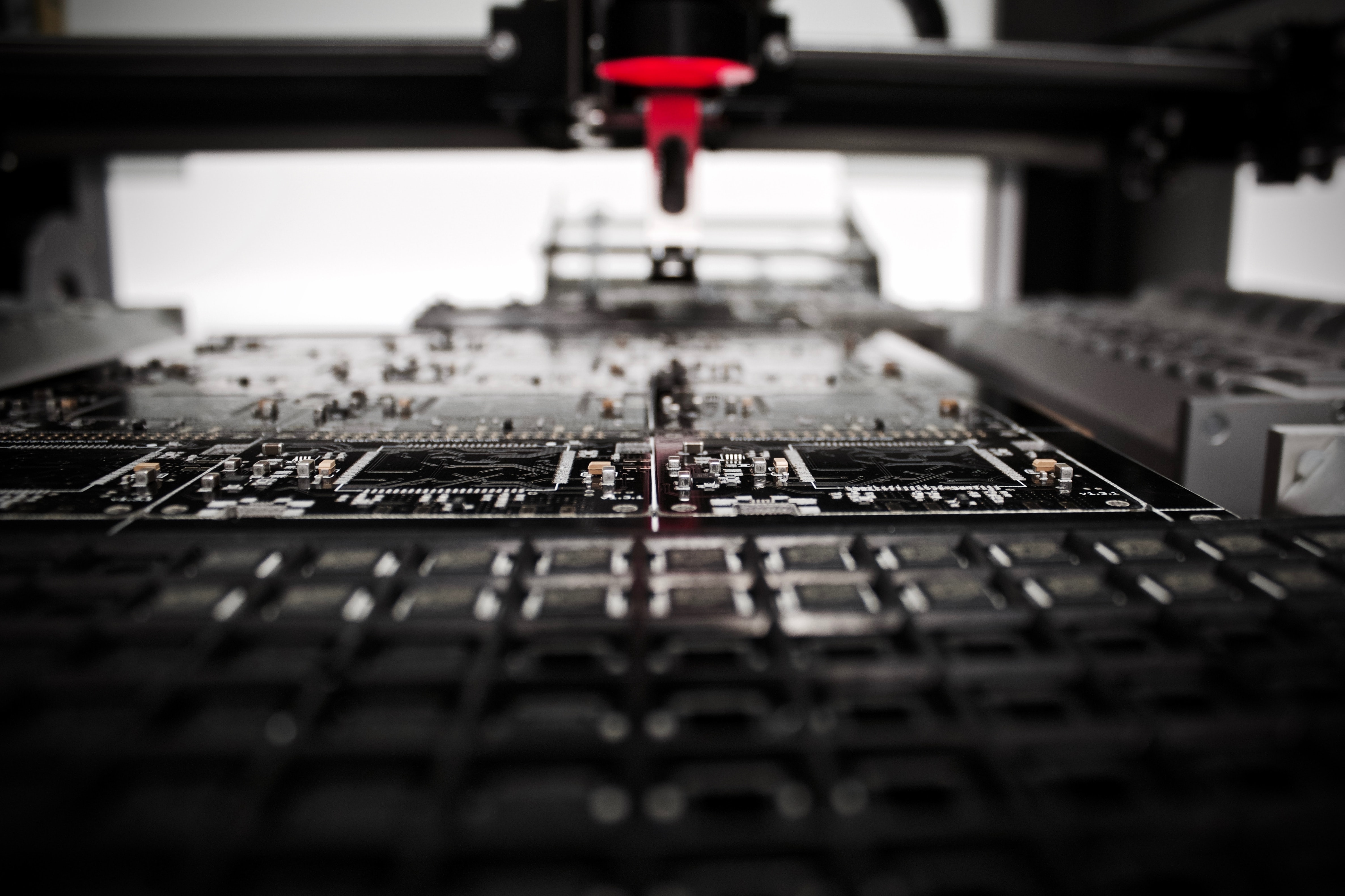
2) Pick and Place Components Mounting
As mentioned before, the assembly of the components on the board is no longer done by hand but through special machines called Pick and Place. These machines are loaded with feeders containing the components that need to be mounted on the PCB. Once the PCB arrives from the soldering machine, a robotic head (or more) begins to pick up the components from the feeders and place them on the PCB. Positioning is done via optical tracking, so the automatic head knows exactly where to go to place the component. These machines can exceed even 100'000 mounted components per hour!
Automatic pick and place machines are mostly used during the SMD assembly process, which deals with small Surface Mount components. In some exceptions, there also exist very specialized automatic PnP machines for THT assembly, so dealing with Through-Hole Components, although this process is still mostly carried on by a human hand.
3) Soldering
Soldering is an extremely delicate process for the quality and correct functioning of the product. In fact, wrong soldering can result in missing connections, short circuits or damage to the PCB which can result in dangerous malfunctions for end customers. The soldering process can be divided in two, depending on whether you are dealing with SMD or THT components. In the first case the reflow soldering is performed. During this process, the PCB runs through a special oven heated following a strategically chosen temperature profile, as some components have certain heat tolerances and may be damaged if the temperature is too high. The solder paste melts around the component's pads and, while cooling, it builds a strong metallic bond between component and PCB.
In the case of THT instead, the wave soldering is performed. Here the PCB with mounted components passes over a hot wave solder tin alloy reservoir. The small "legs" of the THT components catch some liquid tin and while cooling the the same metallic bond explained above is created with the PCB metallic hole. Hemargroup also counts on a selective soldering machine, which can solder specific THT components without having to pass the full board over the liquid. We use it especially in case of mixed THT/SMD double sided boards.
4) Inspection
After each process, it is very important that the PCB is inspected for integrity, proper assembly of components, and correct soldering. This process is performed in 3 ways:
- Optical Inspection: still used in some situations, like after the pick and place phase, it was mostly used in the past or for very small series.
- Automated Optical Inspection (AOI): is performed by machines in a totally automated way, precision and efficiency are maximized.
- X-Ray Inspection: used on PCBs with complex, multi-layer designs or with special components
If the PCB does not pass inspection, it is either reworked or discarded, depending on the type of error.
5) Post Assembly Inspection and Functional Testing
Once the assembly inspection is complete, the PCBs can be further tested for their functionality. Of course, the testing phase can be more or less complicated, depending on whether the finished product needs to pass more stringent regulations, e.g. medical or military equipment.
A testing procedure at this stage can start from a simple "power-up", e.g. for LED lights, and get more and more complex by adding single component measurements, calibration, programming, functional test of sub-circuits, final functional testing of simulated full product, and so on.
Hemargroup is certified for the production of medical and military equipment, so our processes are already optimized for these sectors.
We hope you enjoyed this brief guide on the PCB Assembly process. Should you have an assembly request or would like more information about Hemargroup, please feel free to contact us: