
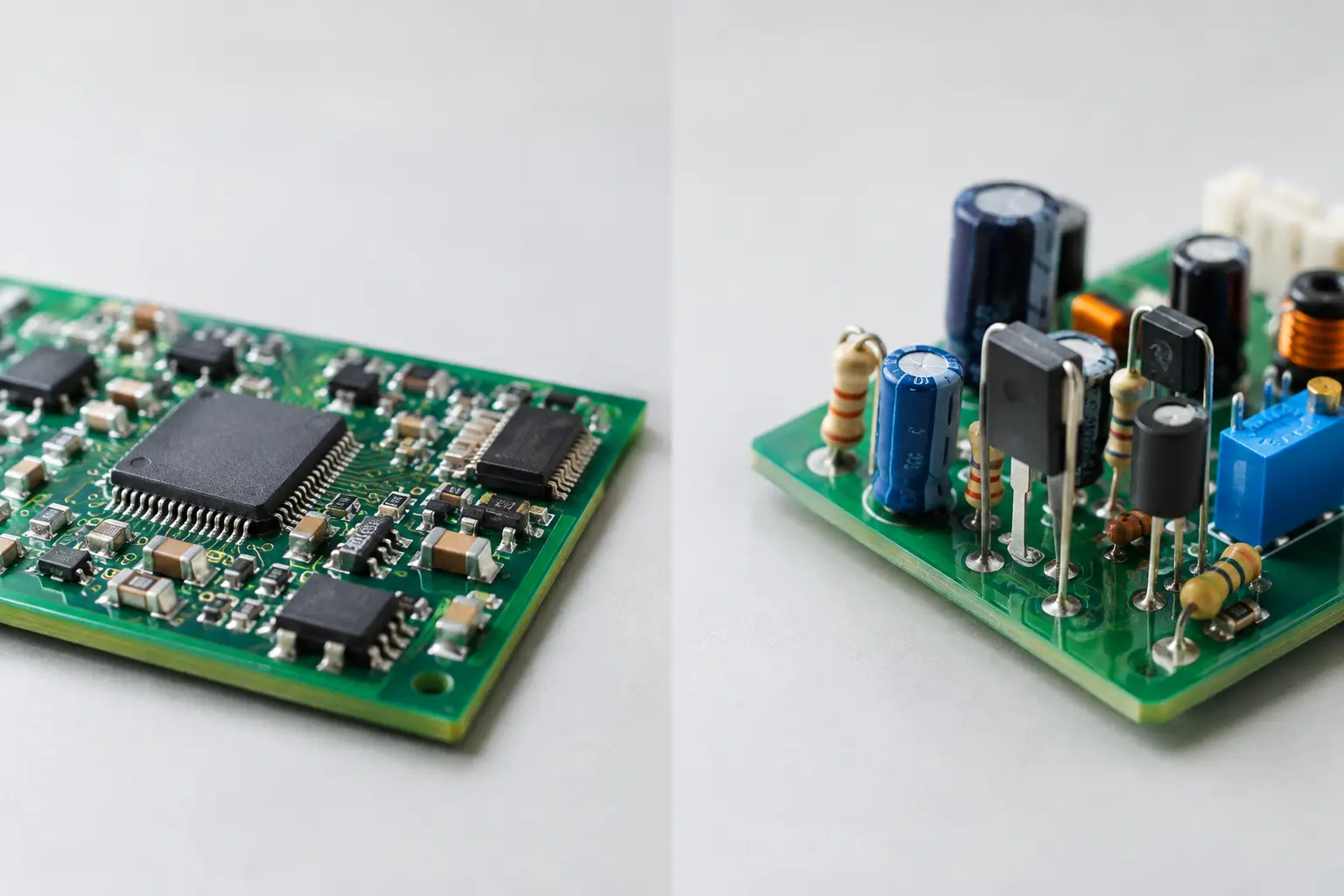
A connector that must withstand repeated handling, a power component that runs hot, and a compact sensor board rarely call for the same assembly method. The decision around SMD versus THT affects PCB layout, component availability, assembly speed, inspection, reliability, product size and long-term manufacturing cost. For product teams, it is not a matter of choosing the newer technology over the older one. It is about selecting the process that supports the real operating conditions of the device.
Surface-mount device assembly and through-hole technology are both established production methods. In many professional products, they are used together on the same PCB. The right choice depends on electrical, mechanical, commercial and lifecycle requirements from the earliest design stage.
SMD versus THT: the practical difference
SMD stands for surface-mount device. Components are placed directly onto pads on the surface of a printed circuit board, then soldered in a reflow oven. Resistors, capacitors, integrated circuits, small transistors and many communication modules are commonly supplied in surface-mount packages.
THT stands for through-hole technology. Component leads pass through drilled holes in the PCB and are soldered on the opposite side, typically by wave soldering, selective soldering or hand soldering. Terminal blocks, large capacitors, high-power devices, switches and connectors are frequent candidates for through-hole mounting.
The distinction seems simple, but its consequences reach beyond the assembly line. SMD generally supports denser circuits and a high degree of automation. THT offers mechanical anchoring through the board and can be more suitable where connectors, heavy components or manual interaction place stress on a solder joint.
Why SMD is the standard for compact electronics
Surface-mount assembly has become the default choice for a large share of modern electronics because it makes efficient use of PCB area. Components can be placed on both sides of the board, while small package sizes allow designers to include more functionality in less space. This is especially valuable in wearables, industrial sensors, communication devices, medical electronics and IoT products where enclosure size matters.
For series production, SMD is also highly automatable. Solder paste printing, optical inspection, automated placement and reflow soldering form a controlled process that can produce large quantities consistently. When a product has a stable design and appropriate component packages, this usually improves throughput and lowers assembly cost per unit.
SMD is not automatically the lowest-cost choice in every situation. A low-volume prototype with a very fine-pitch BGA, for example, may require X-ray inspection, controlled rework capability and specialised process development. The component selection, board complexity and expected production volume must be evaluated together.
Design considerations for SMD
SMD design requires close attention to pad geometry, solder paste apertures, component clearances and the thermal profile of the board. Fine-pitch packages can place demanding requirements on PCB fabrication and placement accuracy. Large thermal pads under power semiconductors may need carefully designed vias and stencil patterns to avoid voids or component floating during reflow.
Component orientation also matters. Consistent orientation supports reliable assembly, inspection and rework. For products exposed to vibration, designers should consider package size, board thickness, mounting points and the location of heavier surface-mount parts. A sound layout is not only electrically correct. It must be manufacturable, testable and serviceable.
Where THT remains the better engineering choice
Through-hole technology remains highly relevant in industrial, power and electromechanical products. Its main advantage is mechanical strength. A connector soldered through the PCB can tolerate more insertion, removal and cable load than many surface-mount alternatives. The same logic applies to switches, relays, transformers and components with substantial mass.
THT can also be preferred for high-power applications. Larger leaded components may provide useful spacing for heat dissipation and electrical isolation. In products where creepage and clearance distances are critical, the physical geometry of through-hole parts can support a safer, more practical layout.
For low-volume builds, THT may simplify certain stages of development. Some parts are easier to probe, replace or adapt manually during early prototype iterations. That does not mean THT is always faster for prototypes. Manual placement and soldering become labour-intensive as component counts increase, and drilled holes add cost and routing constraints to the PCB.
THT constraints to account for early
Every through-hole component consumes board area on both sides. Its holes reduce the space available for signal routing and may limit the use of compact multilayer designs. Drilling, component insertion and selective soldering add process steps that need to be considered when the product is intended for volume production.
Lead spacing, component height and solder-side clearance are equally important. A mechanically strong connector may create assembly challenges if nearby SMD parts obstruct the soldering process. The PCB must be designed around the intended production method rather than treated as an electrical drawing that manufacturing will somehow accommodate later.
Mixed technology is often the best answer
Many successful electronic products use SMD and THT on the same assembly. A typical industrial control board may use SMD for microcontrollers, memory, passives and communication circuits, while retaining THT for power terminals, relays, electrolytic capacitors and user-operated controls.
This mixed approach gives designers the density and automation benefits of SMD without compromising mechanical performance where it matters. It does require production planning. The sequence of soldering operations, component keep-out zones, board support during reflow and inspection access need to be defined before release.
Mixed assembly can involve reflow soldering for surface-mount components followed by selective soldering for through-hole parts. In lower volumes or for complex boards, qualified manual operations may be appropriate. The objective is not to force every product through one standard process. It is to establish a repeatable process that protects quality, traceability and delivery commitments.
Cost is more than the assembly price
When comparing SMD versus THT, unit assembly cost is only one part of the calculation. SMD may reduce board size and support faster placement, but it can increase sensitivity to package availability, stencil quality, moisture handling and inspection requirements. THT may make a board larger and require more manual work, yet avoid a costly mechanical redesign or field failure caused by an unsuitable connector mounting method.
The more useful question is: what is the total cost over the product lifecycle? This includes engineering time, PCB layers, test fixtures, yield, component sourcing, repair, certification needs, production volume and expected service life.
A product intended for a 50-unit pilot run may justify a different package strategy from one planned for 50,000 units annually. The same is true for a device that will be installed once in a protected enclosure compared with equipment that faces vibration, temperature cycles, service access and frequent cable changes in the field.
Reliability, inspection and repair
Both SMD and THT can be highly reliable when the product and process are designed correctly. Reliability does not come from the technology label alone. It comes from proper component selection, correct soldering profiles, controlled materials, inspection and testing aligned with the application.
SMD assemblies are well suited to automated optical inspection, solder paste inspection and, where required, X-ray inspection for hidden joints. THT solder joints can be visually inspected effectively, although dense board designs and certain connector geometries may require additional process controls.
Repairability should be discussed early, particularly for long-life industrial products. Through-hole parts can sometimes be easier to replace, but multi-pin connectors can still require skilled rework. Fine-pitch surface-mount components can be repaired reliably with the right equipment and trained operators, though repeated rework may affect surrounding components or the PCB itself. A repair strategy should be part of industrialisation, not an afterthought once units are in the field.
Make the choice during engineering, not after layout
The best time to decide between SMD, THT or a mixed assembly is while schematic, mechanical constraints and sourcing options are still open. Engineering teams should review how the product will be used, mounted, tested, assembled, transported and serviced. Procurement should assess the lifecycle outlook of proposed packages and approved alternatives. Manufacturing should review the layout for placement, soldering, inspection and panelisation risks.
This is where an integrated EMS partner adds practical value. At Hemargroup, engineering, sourcing and production perspectives can be brought together before design decisions become expensive changes. That supports a clearer route from prototype and 0-series builds to controlled series production.
The right assembly technology is the one that makes the whole product more dependable - not merely the PCB more compact or the first build less expensive. Bring the manufacturing conversation into the design review early, and the final device will be easier to produce, test, scale and support for years.