.png)
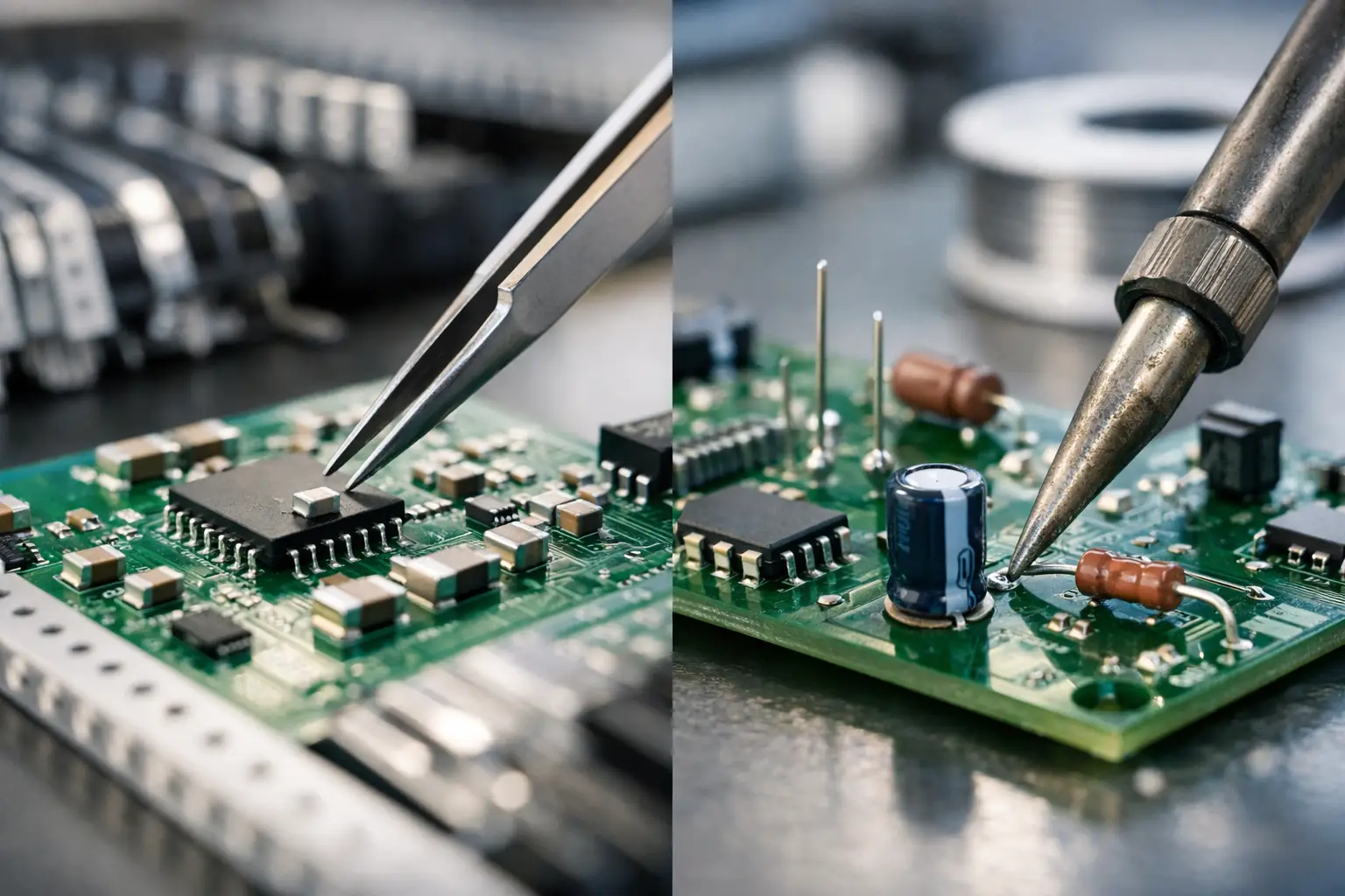
A PCB can look complete on screen yet become difficult, costly or unreliable to manufacture if its components do not match the intended production process. SMD and THT assembly are not competing labels for the same job. They are complementary technologies, each with different consequences for board layout, mechanical strength, test strategy, lead time and production cost.
For product teams, the right question is rarely, “Which method is better?” It is, “Which combination gives this product the required reliability, performance and scalability?” The answer should be made early, ideally while the circuit, PCB layout and enclosure are still being developed. This prevents late redesigns when a prototype moves towards series production.
What SMD and THT assembly mean
Surface-mount device (SMD) assembly places components directly onto pads on the PCB surface. Solder paste is printed through a stencil, components are positioned by automated pick-and-place equipment, and the board passes through a controlled reflow oven. This method supports high component density, compact products and efficient automated production.
Through-hole technology (THT) assembly inserts component leads through holes in the PCB. The leads are soldered on the opposite side, commonly with wave soldering, selective soldering or manual soldering. THT remains valuable where components must tolerate mechanical loads, high currents or repeated connection cycles.
Most professional electronics use both methods. A control board may contain densely packed SMD integrated circuits, resistors and capacitors, while its mains connector, relay, transformer, terminal block or large electrolytic capacitor is mounted using THT. The aim is not to force every component into one process. It is to use the process that best serves the component’s electrical, thermal and mechanical role.
Where SMD assembly delivers value
SMD assembly is the natural choice when product size, component density or production efficiency matters. Modern microcontrollers, memory devices, RF modules and fine-pitch ICs are generally designed for surface mounting. SMD also makes it possible to place components on both PCB sides, reducing the board area required for complex functions.
Automation is a major advantage. Once a design is prepared for manufacture and the component data is verified, pick-and-place systems can position large numbers of parts accurately and consistently. Reflow profiles can be controlled and documented, supporting repeatability across batches. For a product progressing from an initial 0-series to regular production, that consistency is often more valuable than the apparent speed of the first hand-built prototype.
There are trade-offs. Fine-pitch packages, bottom-terminated components and ball grid arrays require careful footprint design, paste-aperture definition and inspection planning. Small passive components can be efficient to assemble, but they are less forgiving of poorly controlled solder paste or unsuitable pad geometry. SMD boards can also be harder to rework when a component is positioned beneath a shield or close to heat-sensitive parts.
A suitable SMD process therefore starts before the production floor. The bill of materials, PCB files, centroid data and component package information must agree. Engineers should also consider component availability, approved alternatives and the risk of end-of-life notifications. A board designed around one difficult-to-source package may create a supply-chain problem long after it has passed its first functional test.
SMD design considerations that avoid delays
PCB layout should provide adequate spacing for placement heads, soldering and optical inspection. Component orientation should be consistent where possible, especially for polarised devices and parts that pass through automated inspection. Fiducials, tooling features and clear polarity markings help maintain process control.
Thermal design requires equal attention. Large copper areas can draw heat away from pads and lead to insufficient solder joints if the footprint is not designed correctly. Thermal reliefs, via placement and the reflow profile all affect the result. For power electronics, the relationship between solder joint quality and heat dissipation should be assessed as part of the complete design, not after initial failures appear.
When THT assembly remains the right choice
THT is often selected for strength and serviceability rather than miniaturisation. A connector that is plugged and unplugged frequently transfers force into the PCB. Leads passing through the board provide a stronger mechanical anchor than many surface-mounted alternatives. The same principle applies to heavy components, high-power devices and parts that may be subject to vibration.
THT can also be appropriate in products where manual assembly or later replacement is expected. Industrial equipment, laboratory devices and long-lifecycle control systems may use terminal blocks, switches, relays or serviceable power components that benefit from through-hole mounting. This does not make THT automatically more reliable. Reliability still depends on the component selection, solder quality, PCB material, environment and product design. It does mean the method can provide a clear advantage under the right mechanical conditions.
The production constraints are different from SMD. Through-hole insertion can be automated for suitable parts, but many projects need manual insertion because of varied component shapes or lower volumes. Wave soldering is efficient for compatible layouts, while selective soldering provides precision for mixed-technology boards and areas that must be protected from excessive heat. Manual soldering remains useful for prototypes, low-volume variants and specialised rework, provided it is performed within defined process controls.
THT layout needs room for the process
Hole size, lead diameter, annular ring dimensions and component keep-out zones must be designed correctly. A hole that appears acceptable in CAD can create insertion or solder-fill issues in production. Components on the solder side may require protection during wave soldering, while tall parts can affect conveyor handling and fixture design.
For mixed boards, the sequence matters. SMD components are usually reflowed first, followed by THT insertion and soldering. That sequence affects which components can be placed on each side of the PCB, the choice of soldering method and whether pallets or dedicated fixtures are required. These details are manageable, but they should be resolved during industrialisation rather than discovered during a production run.
Choosing the right process for the product
The right choice depends on more than annual volume. A compact wearable device will normally favour SMD because space and battery efficiency are limited. A control unit installed in a machine may combine SMD electronics with THT connectors and power components to withstand installation forces and operating vibration. A medical, industrial or transport-related product may require additional traceability, inspection records and test coverage regardless of the assembly technology used.
Cost must be considered across the product lifecycle. SMD can lower the unit cost of repeatable volume production, but it may require investment in stencil preparation, programming and process validation. THT can suit low-volume or mechanically demanding designs, but manual insertion and soldering can increase labour content. A lower assembly price does not help if it creates higher field-failure, repair or sourcing costs later.
A dependable manufacturing partner will review the design in the context of the intended product. That includes expected volumes, sourcing risks, component substitutions, inspection requirements, functional test access, enclosure constraints and anticipated service needs. The best production route may differ between a prototype batch and a stable series build, but the transition should be planned rather than improvised.
Quality control is built into the process
Good solder joints are necessary, but they are not the whole quality plan. Assembly quality begins with controlled incoming materials, verified component references and correct storage conditions for moisture-sensitive devices. It continues through solder paste inspection, placement verification, reflow or soldering controls and optical inspection.
Automated optical inspection can identify missing, misplaced, incorrectly polarised or visibly defective SMD components. X-ray inspection may be required for hidden joints, such as ball grid arrays or bottom-terminated packages. For THT, inspection checks solder fill, lead protrusion, polarity and correct component seating. Visual checks remain valuable, especially for connectors, mechanical parts and product-specific workmanship requirements.
Electrical testing completes the picture. Depending on the product, this can include in-circuit testing, programmed functional testing, boundary scan, calibration or final device testing. Test points should be considered in the PCB layout from the start. If a board cannot be contacted safely and repeatably, production testing becomes slower, more expensive and less effective.
Traceability is equally relevant for products with regulated, industrial or long-life requirements. Recording material lots, process data, inspection outcomes and test results makes it easier to investigate deviations and manage service cases. For complex devices, assembly, programming, mechanical integration and final test should form one controlled flow rather than separate handovers.
From prototype to scalable production
A prototype proves that an idea can work. Industrialisation proves that it can be built repeatedly, inspected efficiently and supplied with controlled risk. The gap between those stages is where many projects lose time.
Before scaling, the design should undergo a manufacturability review covering component availability, alternate parts, panelisation, soldering approach, test fixtures, programming method and packaging requirements. Early prototype quantities may justify a flexible manual process. As demand grows, documented work instructions, fixtures and automated inspection become increasingly valuable.
Hemargroup supports this transition by connecting engineering, procurement, PCB assembly, testing, logistics and lifecycle services within one coordinated process. For customers, this reduces the risk of technical information being lost between a design office, a component broker and a production site. It also gives the project team a clearer route for changes, rework and production ramp-up.
The most useful next step is to review your PCB before the design is frozen. A short discussion about component technology, test access, mechanical loading and expected volumes can prevent a costly change later and give your product a sound route from first build to reliable series production.